CSR
Management Philosophy
"Giving shape to dreams"
We are committed to the challenge of Clean innovation
in response to our customers' needs.
We will shape dreams, surprises, excitement, and the future.
Everything is loved by the world as a partner
* What is "Clean Innovation"* Initiatives that our products, technologies, quality, and environment should always be "clean"
Sustainable Policy
1. Products
Together with our customers and partners, we will create technologies to solve social and environmental issues, enhance the value of people's lives around the world, and aim for the future of a sustainable earth and the development of society.
2. Cooperation with local communities and employees.
We provide all employees who share their management philosophy with opportunities for dialogue, a comfortable work environment, and a place for growth. In addition, we respect diverse cultures and values, take issues seriously, and contribute to the development of the local community.
3. Supply Chain
We will promote CSR procurement together with suppliers, taking into consideration the impact of our business activities on society and the environment.
4. Human Resource Development and Innovation
We foster an internal culture in which diverse people can maximize their abilities and expertise and make the most of each other' lives. We will also provide opportunities to develop human resources to challenge the transformation of innovative markets to solve global issues.
5. Environment
In order to achieve business development through the creation of environmental value with the aim of realizing a sustainable society, we will comply with the requirements applied through our business activities, improve environmental issues, and expand our environmental initiatives with sympathy from people in society.
Sustainability refers to the idea of making the world sustainable from three broad perspectives: environment, society, and economy.
Management, Quality and Environmental Targets
1. Reduce complaints and human error with "clean" quality
- Reduction of external complaints
- Reduction of internal complaints
- Reduction of F costs
- Reduction of human error
2. Controlling CO2 emissions by working on SDGs (reducing wasteful raw materials and energy resources, improving work efficiency without waste and unevenness) in a "Kirei" environment
- Reduction of raw material usage (low money, small Ni, etc.)
- Reduction or maintenance of energy resource consumption (water, electricity, heavy oil, city gas)
- Reduction or maintenance of waste emissions
- Non-use of minerals, etc. in conflict zones
- Proposal of improvement in work efficiency by ingenuity
- Review of wasteful mechanisms (review of heavy management, efficiency of mechanisms, simplification, and efficiency in IT)
3.Materialize and embody "be kind to people and take good care of others"
- Creating a safe and secure work environment
- We will utilize the Safety and Health Committee and safety patrols to create an environment that never causes workers’ compensation, accidents (chemical accidents, pollution control), or fires.
- Thorough 5S3T (thorough cleaning, removal of crystals, contact polishing, cutting debris cleaning, measures against garbage and Garbage fluff, maintenance and maintenance of production facilities)
- Responsibility as a chemical company Thorough maintenance and maintenance in environmental equipment
- Strengthening the utilization of human resources
- Bottom-up of employee skills (skill-up education, multi-skilled workers)
- Appointment of female human resources
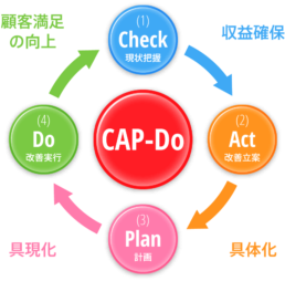
Initiatives for Management, Quality, and Environmental Targets
In order to achieve management, quality, and environmental targets (MS targets), the project team, each department of each office, and the staff department formulate an execution plan to fulfill a given role and carry out initiatives.
Response to conflict minerals
It is said that some of the minerals produced in the Democratic Republic of the Congo and the surrounding countries (DRC countries) are the source of funds for armed groups that perform inhumane acts. Among them, the “Financial Regulation Reform Act” (Dodd-Frank Act) was enacted in July 2010, and in Article 1502, columbite-tantalite (tantalum) and tin stone (tin) were used as conflict minerals (conflict minerals). ), gold and iron manganese heavies (tungsten) are listed, and US listed companies are required to disclose the usage status.
While international efforts are being made to address the above, the Yamato Denki Group will work to eliminate the use of conflict minerals in order to fulfill its social responsibility as a company in the supply chain.
Policy
We do not use conflict minerals that lead to inhumane activities.
If a material procurement investigation reveals that it is a conflict mineral, we will immediately stop trading.
We do not use conflict minerals that lead to inhumane activities. If it is found to be a material that is not limited to conflict minerals and that leads to inhumane activities, we will stop using it immediately.
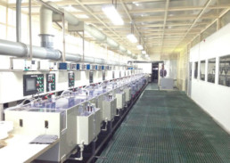
Machining
Machinig and production equipments
Machining
Small lots for quick delivery of product types and number of machines owned by the many Metal (aluminum, iron, SUS system in general, titanium), and a variety of materials for processing resins 5Axis machines , corresponding to the goods polyhedral structure.
Suwa local strengths , cooperation with neighboring manufacturer, supports a variety of processing (laser, sheet metal, printing, heat treatment, polishing, painting, etc.).
Surface manufacturers strengths , corresponding to various surface treatment design and manufacture of parts compatible.
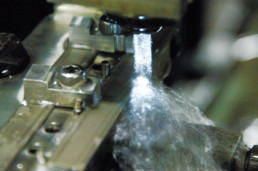
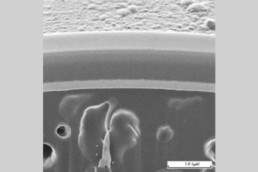
Example: 5axis machining
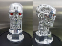
Demonstration ~T2 scalp~
Machine:Mazak Variaxis630 5XⅡ
CAD/CAM: MasterCAM XⅡ
Machining time 18H
Production equipment
Shortening produced by processing in-house sourcing (for short time) can be low cost and when changing the design , in the short term additional machining of fine-tuning during assembly, parts procurement available.
Production Drawing from your concept, improving existing equipment and parts production and assembly drawings to accommodate your various needs flexibly.
Separator for the mixture of Steel ball and chip devices
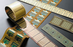
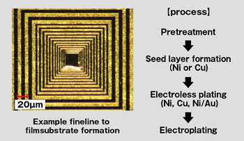
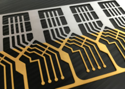
Plating for Microelectronics
Plating of electronics substrate and devices for microelectronics
Electroless Au plating for fineline circuit on PC board
(L/S = 30/30µm)
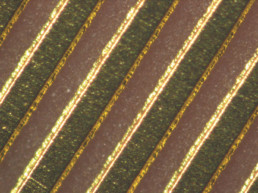
Electroless Ni/Pd/Au plating for micro-circuit
Excellent soldering, wirebondability. 3layers plating:Ni/Pd/Au is improved surface mounting reliability.
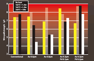
Au Wire pull test
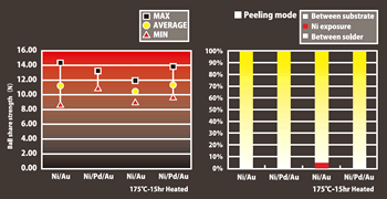
Ball share test
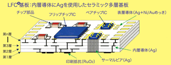
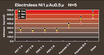
Au Plating for LTCC substrate
Electroless plating process for LTCC substrate silver electrode
Wire pull strength on thicktype electroless Au plating film
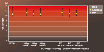
Electrode: Electroless plating on Ag/Pt
Plating thickness: Ni3μm Au0.4μm N=50
Au wire: 30μmφ Bonder: Kaijo118CH (Full auto type)
Gold plating for electroless wire bonding for semiconductor wafers
In recent years, while UBM formation (Under Bump Metal) by electroless plating on semiconductor wafer mounting pad electrodes has attracted attention, we have cultivated for many years, utilizing the gold plating technology for printed circuit boards used in SMD, etc., it is possible to process electroless gold plating for stable wire bonding.
Even wafers with a mixture of SR and polyimides can be selectively bonded gold plating on the pad.
| Plating Process | Plating Thickness | Wafer Size | Wafer Thickness | Pad | Pad Size |
| ENIG (Eletroless Ni/F-Au) | Ni:0.5~10um Pd:0.02~0.8um Au:0.02~0.8um | Small pieces ~8inch *10 inches can be prototyped | 300um~2mm ※300um or less Wafer reinforced by tape as needed | Al | φ10um~ Plating support possible |
| ENIGAG (Electroless Ni/Thick-Au) | Al-Si | ||||
| ENEPIG (Electroless Ni/Pd/F-Au) | Al-Si-Cu | ||||
| ENEPIGAG (Electroless Ni/Pd/Thick Au) | Al-Cu | ||||
| Cu |
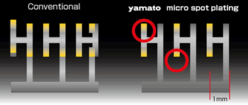
Micro spot plating for micro connector
Spot plating is plated with technology only where necessary.
Can significantly reduce the amount of use Au.
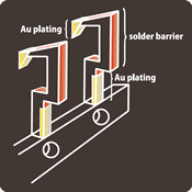
Material: Cu alloy
Material Thicness: 0.08mm~
Material width: ~20mm
Plathing thicness: Ni 1μm~ Au0.1~0.5μm
Solder Barrier area: 0.3mm~
Method of forming a Solder Barrier : Lazer or special masking
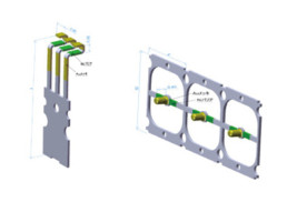
Example of Spot Plating
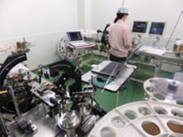
Visual Inspection System by in-house production
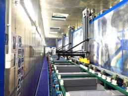
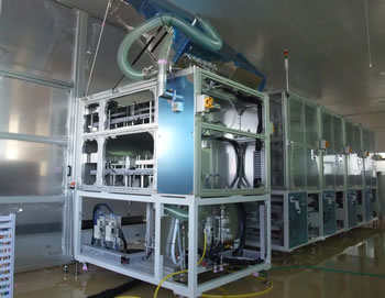
Reel to reel plating for presses devices for automotive applications
| Transport | By vertical transport, both single-tie bar and center carrier are possible. |
| Product shape | Materials, primary pressed both possible |
| The material amplitude | tandard Max100mmW *Consultation for more cases |
| Material thickness | Standard Max0.8mmt *Consultation for no more |
| Others | Consultation on mixed specifications of stripe and spot plating, stripe plating (±0.1 mm), etc. |
Four color plating
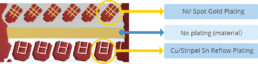
Reflow tin plating with each different thickness
Spot plating

Sn reflow plating for automotive press-fit terminals

The temperature profile of the reflow is checked by the initial condition setting, and the pure tin thickness and the diffusion layer thickness are controlled. If necessary, we perform cross-sectional observation by CP and IM to ensure the plating layer structure.
Pb free plating
Reflow tin plating
Tin plating is used as an alternative to leadcontaining solder plating. It is necessary to take a measure for whisker. Internal stress of crystal particles which causes whiker can be eased by reflowing process. We produce reflow tin plating for connector in volume.
Before reflow
After reflow
Surface of reflow tin

Before reflow
After reflow
Before reflow

After reflow
Zero-cross time (second)
| After plating | PCT: 5hrs | PCT: 16hrs | ||||
| Before reflow | After reflow | Before reflow | After reflow | Before reflow | After reflow | |
| 1 | 0.33 | 0.80 | 0.47 | 0.70 | 0.58 | 1.08 |
| 2 | 0.43 | 0.70 | 0.42 | 0.80 | 0.51 | 1.36 |
| 3 | 0.32 | 0.69 | 0.40 | 0.93 | 0.48 | 1.50 |
| 4 | 0.32 | 0.71 | 0.50 | 0.95 | 0.30 | 1.04 |
| 5 | 0.35 | 0.44 | 0.63 | 1.16 | 0.43 | 1.48 |
| AVE. | 0.35 | 0.67 | 0.48 | 0.91 | 0.46 | 1.29 |
| MAX. | 0.43 | 1.80 | 0.63 | 1.16 | 0.58 | 1.50 |
| Min. | 0.32 | 0.44 | 0.40 | 0.70 | 0.30 | 1.04 |
| STD. | 0.05 | 0.13 | 0.09 | 0.17 | 0.10 | 0.22 |
Measurement: SWET-2000 / Sn-3Ag-0.5Cu Solder / Rosin flux
PCT: 121℃-100℃RH
Reflow tin whiskers
Cu/Sn 1μm
46 days later
Non-reflow
After reflow
4 months later
Non-reflow
After reflow
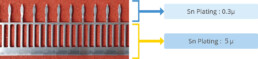
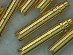
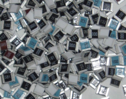
Barrel Plating
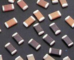
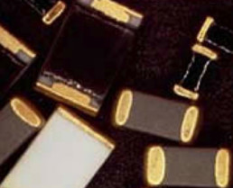
| Products | A | Chip resistor, Chip capacitor, Chip inductor, Chip filter, SMD products by chip type |
| B | Small stamping parts | |
| Size | A | min 1.0mm × 0.5mm ~ |
| B | Pin: min ø0.5mm × 2mm ~ Plate: min 2.0mm × 1.5mm ~ | |
| Plating Thickness | A | Electrolytic Ni, Sn or Au |
| B | Electroless Ni, Electro Ni / Electro Au, Electro Ni / Electro Sn, Electro Ni / Electro Ag, Electro Cu |
A) Possible to plate various chip size devices with flexible treatment.
B) Possible to plating small parts with various kind of plating.
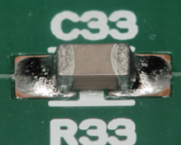
Gold plating for small connector parts
Tin plating to chip device
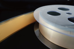
Plating on Metal foil
Continuous Ni and Au plating are possible for Cu, stainless steel foil material with the thinnest 10μm thick. (Maximum width 160mm)
It can be used as a reinforcing substrate for battery materials and flexible substrates.
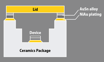
It is possible to form wax materials with gold tin, silver tin, and silver copper by plating method to 30μm thick kovar material.
It is used as a sealing material such as ceramic packages.
| Material Thickness | Plating | Plating Thickness | |
| Kovar | 10μm | Au80/Sn20 | 4~20μm |
| Ag/Sn5 | ~200μm | ||
| Ag/Cu | 4μm~ | ||
| SUS・Cu | Ni・Au | 1μm~ | |
| Film with Cu | 20μm~ | Ni/Au | 1μm/0.1μm~ |
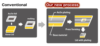
Gold Tin Alloys by plating forming for Brazing assembly
Can form the plating material is used in brazing electronic packaging devices.
80Au/20Sn alloys by plating forming.
Comparison of plating with rolling foil
| plating | traditinal | |
| Oxdation | ○ | ○ |
| Base material selection | ○ | △ |
| Out gas | ○ | ○ |
| wettability | ○ | ○ |
| Thicness control | ◎ | △ |
| cost | ○ | △ |
| Ratio control | ○ | △ |
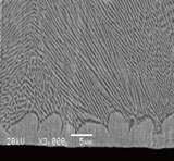
Molten state of plating Au80/Sn20
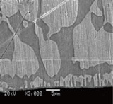
Molten state of Traditional brazing
New technology of plating for microelectronics
Etching free plating without using roughned process
Direct plating of organic film material
Traditionally, when film formation to maintain smooth as glass and plastic, been using dry process is expensive.
Maintaining surface smoothness of the material, can form a solid film by this new plating process.
Maintain the smoothness of nanoscale.
Without using a dry process, polyimide,glass,PET, PEN ,PPA, LCP, Polycarbonate plating can be formed into high performance and lowcost.
Can also ITO electrode plating thicktype electroless Au.
Direct plating on glass
Usually, direct plating to glass strongly roughs the glass surface with hydrofluoric acid, etc., but in our development process, it is possible to form a plating film with mirror gloss by adopting a unique pretreatment that hardly devastates the material and a unique electroless plating with high uniformity.
Electroless Cu plating
Appearance surface roughness after plating
Our pretreatment, which hardly devastates the material, allows the surface roughness of the nano-order to form a high-adhesion plating film.
Before Pre-treatment Ra: 0.5nm
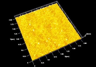
After pretreatment Ra: 1nm
Zinc-free plating on aluminum
Usually, aluminum materials are highly solubility in acids and alkalis, and it is common to chemically perform zinc substitution (zinc treatment) and perform plating processing.
This technology is capable of plating directly into aluminum materials without zinc replacement treatment.
As a result, the process is shortened, and the partial plating method can be easily performed.
Process
Preprocessing
↓
Material etching
↓
Au Strike Plating
↓
Bondable Au plating
Example of direct gold plating for aluminum lead frame
Material: A1020P.
Au plating thickness: 1μm (stripe plating)
Plating to non-woven fabric
It is a technology to uniformly coat various plating coatings to fibers such as non-woven fabric.
Material: Poliolephin
Ni plating thickness: 0.1μm~
Material: Polyester
Ni plating thickness: 0.1μm~
FIB SIM
Material: PP weaving.
Sn plating thickness: 0.5μm~
FIB SIM
Cross-section EDS mapping
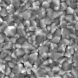
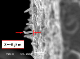
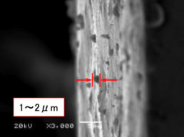
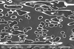
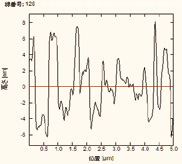
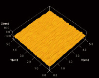
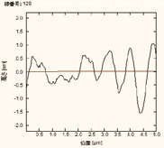
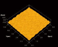
Roughed Ni plating
Nickel plating with an increased surface area by roughing the plating film can be produced for applications such as improving adhesion to resins. The entire surface is uneven and the Rz is over 2.0 μm.
FE-SEM secondary electron image (40° tilt)
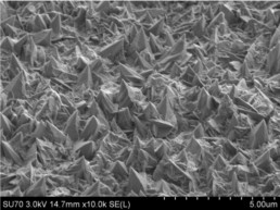
Example of coarsened nickel plating
Material: Copper plate
Ni plating thickness: 5.0μm~
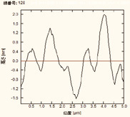
Unevenness measurement (laser microscope)
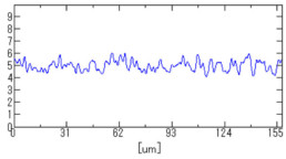
Roughness measurement results
Ra 0.31um
Rz 2.04um
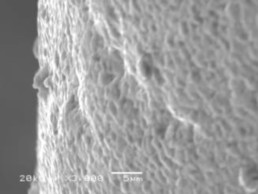
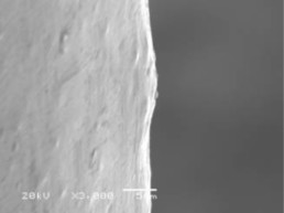
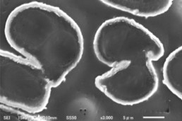
Direct plating for titanium and SUS
Gold plating and nickel plating are possible directly on titanium, which is represented by difficult-to-plating materials. There is no defect between the material and the plating, and the adhesion is good. In addition, copper plating with good direct adhesion on SUS also possible.
FIB SIM image
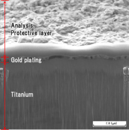
Example of direct gold plating for titanium
Material: Titanium
Au plating thickness: 0.2μm~
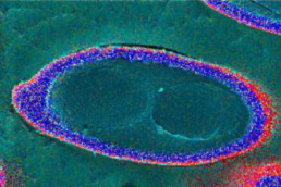
FIB SIM image
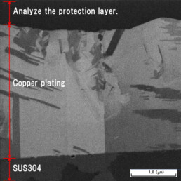
Example of direct copper plating of stainless steel
Material: SUS304
Cu plating thickness: 3.0μm~
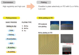
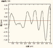
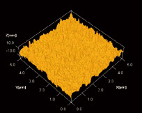
Electroless plating on ITO electrade
Roughness if surface on ITO and glass substrate after etching
ITO: Before etching
Ra: 0.65nm Rz: 3.62nm
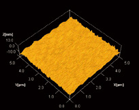
ITO: After etching
Ra: 2.78nm Rz: 14.37nm
Glass: Before etching
Ra: 0.35nm Rz: 1.84nm
Glass: After etching
Ra: 0.42nm Rz: 2.25nm
By etching ITO selectively, the surface of glass has not changed while the ITO surface gets four times rough.
Company Overview
Introduction of Yamato
Company Profile
| President & CEO | Masahiro Hara |
| Capital | 90million JPY |
| Established | 27/Apl/1944 |
| Employee | 410 |
| Product Items | ● Plating for micro-electronics devices, substrates and various materials. ● Machining works for tools and metal parts ● Machinery design and manufacture |
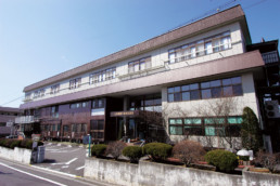
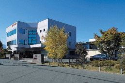
Head office
Shimosuwa
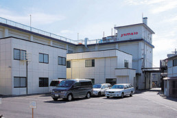
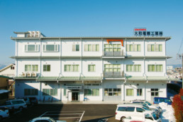
Suwa and R&D
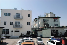
Matsumoto
Kohki Div
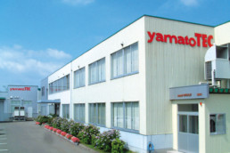
YamatoTEC
History
| Apr/1944 | Established in 5312 Shimosuwa,Nagano |
| Jun/1970 | Constructed Shimosuwa |
| Oct/1970 | Constructed Matsumoto |
| Mar/1977 | Constructed SUWA |
| Aug/1983 | Constructed Head office building |
| Aug/1989 | Established YamatoTEC |
| Dec/1996 | Registrated ISO9002 |
| Mar/2000 | Registrated ISO14001 |
| Dec/2002 | Registrated ISO9001#2000 |
| Mar/2005 | Constructed R&D building |
| Mar/2006 | Registrated ISO14001#2004 |
| Sep/2008 | Established Kohki Div.(Machining and equipment Div.) |
| Dec/2008 | Registrated ISO/TS16949:2000 in Matsumoto |
| Oct/2012 | Established Shinsei (Thailand) Co,.LTD |
| Nov/2017 | Mingrated to IATF16949:2016 |
| Dec/2017 | Migrated to ISO2015 ISO9001 :2015/JIS Q 9001:2015 ISO14001 :2015/JIS Q 14001:2015 |
| Jan/2019 | Made Shinsei (Thailand) Co.,LTD a wholly owned subsidiary and changed the company name to Yamato Denki (Thailand) Co., LTD. |
| Jan/2021 | Registrated IATF16949: 2016 certification in Suwa-factory |
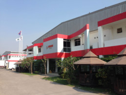
Introduction of Yamato Denki (Thailand)
Company Profile
| Location | 40/17-19 Moo 5 , Rojana Industrial Park , T.U-Thai, A.U-Thai, Ayuttaya Province 13210 |
| Managing Director | Masayuki Nakayama |
| Establishment | Construction 28/JUN/2005 Start business on 6 /Dec /2005 |
| Capital | 50,000,000 THB (150mil.JPY)(Yamato IND 100%) |
| Business | Surface treatment For Microelectronics (HDD & CPU & automobile, Camera etc… ) (Electroless Ni Plating / Electro Ni Plating / Electro Au Plating / Chemical Polishing / Ultra clean wash / etc) |
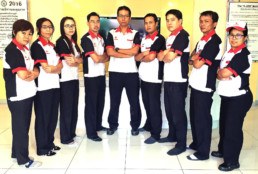
| Employee | 320 persons (Japanese staff 2 persons)as of July 2018 |
| All area | Factory #1 = 5,529㎡ Floor area: 2,250㎡ Factory #2 = 5,550㎡ Floor area: 1,875㎡ Factory #3 = 6,075㎡ Floor area: 2,275㎡ (Including Factory, Waste water treatment area) |
| Other | ISO9001:2008 ISO140001:2004 ISO/TS16949:2009 Certifired * TS16949 will be transferred to IATF16949 on November 2018. |